发布时间:2012-05-23 阅读量:1166 来源: 我爱方案网 作者:
中心议题:
* TI TMS320VC5505 ECG解决方案
TI 公司的ECG解决方案是采用TMS320VC5505 定点DSP,它是基于TMS320C55x DSP CPU核的定点DSP,它的C55x™ DSP架构可得到高性能和低功耗特性,CPU支持内部总线架构,包括一条可编程总线,一条321位数据总总线和两条16位数据读总线,两条数据写总线和专门用于外设和DMA的其它总线. TMS320VC5505还包括4个DMA控制器,每个四路.时钟为60MHz或100MHz,指令周期为16.67ns或10ns.主要用于无线音频设备,回声消除耳机,手提媒体设备,视频,工业控制,指纹生物学和SDR. 本文介绍了TMS320VC5505的主要特性和方框图以及采用TMS320VC5505的ECG解决方案方框图, ECG前端板详细电路图和所用材料清单(BOM).
Basic functions of an ECG machine include ECG waveform display, either through LCD screen or printed paper media, and heart rhythm indication as well as simple user interface through buttons. More features, such as patient record storage through convenient media, wireless/wired transfer and 2D/3D display on large LCD screen with touch screen capabilities, are required in more and more ECG products. Multiple levels of diagnostic capabilities are also assisting doctors and people without specific ECG trainings to understand ECG patterns and their indication of a certain heart condition. After the ECG signal is captured and digitized, it will be sent for display and analysis, which involves further signal processing.
.jpg)
图1.TI ECG方框图
ECG Implementation on the TMS320VC5505 DSP Medical Development Kit (Rev. A)
The TMS320VC5505 is a member of TIs TMS320C5000™ fixed-point Digital Signal Processor (DSP) product family and is designed for low-power applications.
The TMS320VC5505 fixed-point DSP is based on the TMS320C55x™ DSP generation CPU processor core. The C55x™ DSP architecture achieves high performance and low power through increased parallelism and total focus on power savings. The CPU supports an internal bus structure that is composed of one program bus, one 32-bit data read bus and two 16-bit data read buses, two 16-bit data write buses, and additional buses dedicated to peripheral and DMA activity. These buses provide the ability to perform up to four 16-bit data reads and two 16-bit data writes in a single cycle. The TMS320VC5505 also includes four DMA controllers, each with 4 channels, providing data movements for 16-independent channel contexts without CPU intervention. Each DMA controller can perform one 32-bit data transfer per cycle, in parallel and independent of the CPU activity.
The C55x CPU provides two multiply-accumulate (MAC) units, each capable of 17-bit x 17-bit multiplication and a 32-bit add in a single cycle. A central 40-bit arithmetic/logic unit (ALU) is supported by an additional 16-bit ALU. Use of the ALUs is under instruction set control, providing the ability to optimize parallel activity and power consumption. These resources are managed in the Address Unit (AU) and Data Unit (DU) of the C55x CPU.
The C55x CPU supports a variable byte width instruction set for improved code density. The Instruction Unit (IU) performs 32-bit program fetches from internal or external memory and queues instructions for the Program Unit (PU). The Program Unit decodes the instructions, directs tasks to the Address Unit (AU) and Data Unit (DU) resources, and manages the fully protected pipeline. Predictive branching capability avoids pipeline flushes on execution of conditional instructions.
The general-purpose input and output functions along with the 10-bit SAR ADC provide sufficient pins for status, interrupts, and bit I/O for LCD displays, keyboards, and media interfaces. Serial media is supported through two MultiMedia Card/Secure Digital (MMC/SD) peripherals, four Inter-IC Sound (I2S Bus™) modules, one Serial-Port Interface (SPI) with up to 4 chip selects, one I2C multi-master and slave interface, and a Universal Asynchronous Receiver/Transmitter (UART) interface.
The VC5505 peripheral set includes an external memory interface (EMIF) that provides glueless access to asynchronous memories like EPROM, NOR, NAND, and SRAM. Additional peripherals include: a high-speed Universal Serial Bus (USB2.0) device mode only, and a real-time clock (RTC). The DMA controller provides data movement for sixteen independent channel contexts without CPU intervention, providing DMA throughput of up to two 16-bit words per cycle. This device also includesthree general-purpose timers with one configurable as a watchdog timer, and a analog phase-locked loop (APLL) clock generator.
In addition, the VC5505 includes a tightly-coupled FFT Hardware Accelerator. The tightly-coupled FFT Hardware Accelerator supports 8 to 1024-point (in power of 2) real and complex-valued FFTs.
.gif)
.gif)
.gif)
.gif)
.gif)
.gif)
.gif)
.gif)
.gif)
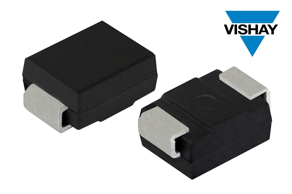
汽车电子系统日益复杂,尤其在48V架构、ADAS与电控系统普及的当下,对瞬态电压抑制器(TVS)的功率密度、高温耐受性及小型化提出了严苛挑战。传统大功率TVS往往体积庞大,难以适应紧凑的ECU布局。威世科技(Vishay)日前推出的T15BxxA/T15BxxCA系列PAR® TVS,以创新封装与卓越性能直面行业痛点,为下一代汽车设计注入强大保护能力。

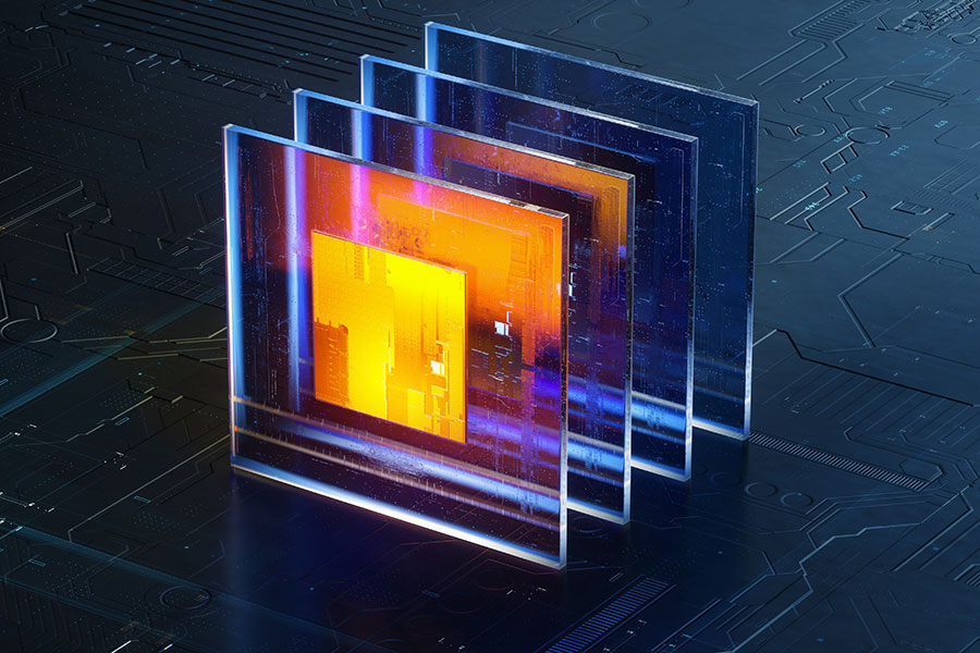
韩国半导体巨头SK海力士近日在DRAM制造领域实现重大技术飞跃。据ZDNet Korea报道,该公司首次在其1c制程节点中成功应用6层EUV(极紫外)光刻技术,显著提升了DDR5与HBM(高带宽内存)产品的性能、密度及良率,进一步巩固其在先进内存市场的领导地位。
半导体封测巨头日月光投控最新财报显示,2024年7月公司实现营收515.42亿元新台币,较6月份环比增长4.1%,与上年同期相比则微降0.1%。若以更能反映国际业务实质的美元计价,7月营收高达17.69亿美元,呈现更强劲的增长势头——环比上升6.5%,同比显著增长11.2%。这一差异突显了新台币汇率波动对账面营收换算带来的影响。
据彭博社8月11日援引知情人士消息,全球动力电池龙头宁德时代(CATL)已正式暂停其位于江西省宜春市的建霞锂矿生产作业,此次停产预计将持续至少三个月。这一重大变动迅速引发锂产业链高度关注。
近日,全球移动芯片两大巨头——中国台湾地区的联发科(MediaTek)与美国的高通(Qualcomm)先后发布了最新一季的财务报告,为洞察消费电子市场动态和半导体产业发展方向提供了重要窗口。两份财报清晰地展现了在智能手机市场增长放缓的背景下,两大巨头正积极寻求多元化突破,竞相布局未来增长引擎。


