发布时间:2012-04-23 阅读量:2689 来源: 我爱方案网 作者:
中心议题:
* Keil ST STM32F407评估开发方案
Keil公司的MCBSTM32F400评估板采用ST公司的STM32F407IG器件,它是基于168MHz ARM Cortex™-M4的MCU,176引脚BGA封装,具有1MB Flash & 192KB RAM,外接存储器8MB NOR Flash, 512MB NAND Flash, 2MB SRAM, 8KB I2C EEPROM,采用电阻触摸屏的2.4吋彩色QVGA TFT LCD,10/100以太网端口,主要用在马达驱动和应用控制,医疗设备,工业应用如PLC,逆变器,电路中断器,打印机和扫描仪,告警系统,视频互连,HVAC以及家庭音响设备.本文介绍了STM32F405xx和STM32F407xx 主要特性,方框图,MCBSTM32F400评估板主要特性,技术指标,方框图以及电路图和PCB元件布局图.
STM32F405xx/STM32F407xx:ARM Cortex-M4 32b MCU+FPU, 210DMIPS, up to 1MB Flash/192+4KB RAM, USB OTG HS/FS, Ethernet, 17 TIMs, 3 ADCs, 15 comm. interfaces & camera
The STM32F405xx and STM32F407xx family is based on the high-performance ARM®Cortex™-M4 32-bit RISC core operating at a frequency of up to 168 MHz. The Cortex-M4core features a Floating point unit (FPU) single precision which supports all ARM singleprecision data-processing instructions and data types. It also implements a full set of DSP instructions and a memory protection unit (MPU) which enhances application security. The Cortex-M4 core with FPU will be referred to as Cortex-M4F throughout this document.
The STM32F405xx and STM32F407xx family incorporates high-speed embedded memories (Flash memory up to 1 Mbyte, up to 192 Kbytes of SRAM), up to 4 Kbytes of backup SRAM, and an extensive range of enhanced I/Os and peripherals connected to two APB buses, two AHB buses and a 32-bit multi-AHB bus matrix.
All devices offer three 12-bit ADCs, two DACs, a low-power RTC, twelve general-purpose 16-bit timers including two PWM timers for motor control, two general-purpose 32-bit timers. a true random number generator (RNG). They also feature standard and advanced communication interfaces.
● Up to three I2Cs
● Three SPIs, two I2Ss full duplex. To achieve audio class accuracy, the I2S peripherals can be clocked via a dedicated internal audio PLL or via an external clock to allow synchronization.
● Four USARTs plus two UARTs
● An USB OTG full-speed and a USB OTG high-speed with full-speed capability (with the ULPI),
● Two CANs
● An SDIO/MMC interface
● Ethernet and the camera interface available on STM32F407xx devices only. New advanced peripherals include an SDIO, an enhanced flexible static memory control (FSMC) interface (for devices offered in packages of 100 pins and more), a camera interface for CMOS sensors.
The STM32F405xx and STM32F407xx family operates in the –40 to +105 °C temperature range from a 1.8 to 3.6 V power supply. The supply voltage can drop to 1.7 V when the device operates in the 0 to 70 °C temperature range and PDR is disabled. A comprehensive set of power-saving mode allows the design of low-power applications.
The STM32F405xx and STM32F407xx family offers devices in four packages ranging from 64 pins to 176 pins. The set of included peripherals changes with the device chosen.
These features make the STM32F405xx and STM32F407xx microcontroller family suitable for a wide range of applications:
STM32F405xx和STM32F407xx 主要应用:
● Motor drive and application control
● Medical equipment
● Industrial applications: PLC, inverters, circuit breakers
● Printers, and scanners
● Alarm systems, video intercom, and HVAC
● Home audio appliances
STM32F405xx和STM32F407xx 主要特性:
■ Core: ARM 32-bit Cortex™-M4 CPU with FPU,Adaptive real-time accelerator (ART Accelerator™) allowing 0-wait state execution from Flash memory, frequency up to 168 MHz, memory protection unit, 210 DMIPS/ 1.25 DMIPS/MHz (Dhrystone 2.1), and DSP Instructions
■ Memories
Up to 1 Mbyte of Flash memory
– Up to 192+4 Kbytes of SRAM including 64-Kbyte of CCM (core coupled memory) data RAM
– Flexible static memory controller supporting Compact Flash, SRAM, PSRAM, NOR and NAND memories
■ LCD parallel interface, 8080/6800 modes
■ Clock, reset and supply management
– 1.8 V to 3.6 V application supply and I/Os
– POR, PDR, PVD and BOR
– 4-to-26 MHz crystal oscillator
– Internal 16 MHz factory-trimmed RC (1% accuracy)
– 32 kHz oscillator for RTC with calibration
– Internal 32 kHz RC with calibration
● Low power
– Sleep, Stop and Standby modes
– VBAT supply for RTC, 20×32 bit backup registers + optional 4 KB backup SRAM
■ 3×12-bit, 2.4 MSPS A/D converters: up to 24 channels and 7.2 MSPS in triple interleaved mode
■ 2×12-bit D/A converters
■ General-purpose DMA: 16-stream DMA controller with FIFOs and burst support
■ Up to 17 timers: up to twelve 16-bit and two 32- bit timers up to 168 MHz, each with up to 4 IC/OC/PWM or pulse counter and quadrature (incremental) encoder input
■ Debug mode
– Serial wire debug (SWD) & JTAG interfaces
– Cortex-M4 Embedded Trace Macrocell™
1. The WLCSP90 package will soon be available.
■ Up to 140 I/O ports with interrupt capability
– Up to 136 fast I/Os up to 84 MHz
– Up to 138 5 V-tolerant I/Os
■ Up to 15 communication interfaces
– Up to 3 × I2C interfaces (SMBus/PMBus)
– Up to 4 USARTs/2 UARTs (10.5 Mbit/s, ISO 7816 interface, LIN, IrDA, modem control)
– Up to 3 SPIs (37.5 Mbits/s), 2 with muxed full-duplex I2S to achieve audio class accuracy via internal audio PLL or external clock
– 2 × CAN interfaces (2.0B Active)
– SDIO interface
■ Advanced connectivity
– USB 2.0 full-speed device/host/OTG controller with on-chip PHY
– USB 2.0 high-speed/full-speed device/host/OTG controller with dedicated DMA, on-chip full-speed PHY and ULPI
– 10/100 Ethernet MAC with dedicated DMA:
supports IEEE 1588v2 hardware, MII/RMII
■ 8- to 14-bit parallel camera interface up to 54 Mbytes/s
■ True random number generator
■ CRC calculation unit
■ 96-bit unique ID
■ RTC: subsecond accuracy, hardware calendar
.gif)
图1.STM32F405xx和STM32F407xx 方框图
MCBSTM32F400评估板
The MCBSTM32F400 Evaluation Board ships with the STM32F407IG device that is a superset of several other device variants of the STM32F407x microcontroller series. The MCBSTM32F200 and MCBSTM32F400 boards contain all the hardware components required in a single-chip STM32x system.
The Keil MCBSTM32F400 Evaluation Board enables you to create and test working programs based on the STMicroelectronics STM32 F4xx series of ARM Cortex™-M4 processor-based devices.
MCBSTM32F400评估板主要特性:
168MHz STM32F407IG ARM Cortex™-M4 processor-based MCU in 176-pin BGA
On-Chip Memory: 1MB Flash & 192KB RAM
External Memory: 8MB NOR Flash, 512MB NAND Flash, 2MB SRAM, 8KB I2C EEPROM with NFC interface
2.4 inch Color QVGA TFT LCD with resistive touchscreen
10/100 Ethernet Port
USB 2.0 Full Speed - USB, USB-OTG, & USB Host
USB 2.0 High Speed - USB, USB-OTG, & USB Host
1 CAN Interface
Serial/UART Port
MicroSD Card Interface
5-position Joystick
3-axis digital Accelerometer
3-axis digital Gyroscope
Analog Voltage Control for ADC Input (potentiometer)
Audio CODEC with Line-In/Out and Speaker/Microphone
Digital Microphone
Digital VGA Camera
Push-Buttons for Reset, Wakeup, Tamper and User
8 LEDs directly connected to port pins
Power Supply via:
High Speed and Full Speed USB (micro) connectors
Power jack (8V-12V) with Voltage Regulator capable to supply both USB host interfaces (500mA each)
Debug Interface Connectors
20 pin JTAG (0.1 inch connector)
10 pin Cortex debug (0.05 inch connector)
20-pin Cortex debug + ETM Trace (0.05 inch connector)
.jpg)
图2.MCBSTM32F400评估板外形图
The MCBSTM32F200 and MCBSTM32F400 use the same base board and on-chip peripherals. Only the MCU is different between the two boards.
The hardware block diagram displays the input, configuration, power system, and User I/O on the board. This visual presentation helps you to understand the MCBSTM32F200 board components.
.gif)
图3.MCBSTM32F400评估板方框图
.gif)
图4.MCBSTM32F400评估板电路图(1)
.gif)
图5.MCBSTM32F400评估板电路图(2)
.gif)
图6.MCBSTM32F400评估板电路图(3)
.gif)
图7.MCBSTM32F400评估板电路图(4)
.gif)
图8.MCBSTM32F400评估板电路图(5)
.gif)
图9.MCBSTM32F400评估板电路图(6)
.gif)
图10.MCBSTM32F400评估板电路图(7)
.gif)
图11.MCBSTM32F400评估板电路图(8)
.gif)
图12.MCBSTM32F400评估板电路图(9)
.gif)
图13.MCBSTM32F400评估板电路图(10)
.gif)
图14.MCBSTM32F400评估板电路图(11)
.gif)
图15.MCBSTM32F400评估板电路图(12)
.gif)
图16.MCBSTM32F400评估板元件布局图(1)
.gif)
图17.MCBSTM32F400评估板元件布局图(2)
.gif)
图18.MCBSTM32F400评估板元件布局图(3)

在AIoT技术加速赋能全球数字化转型、中国持续引领物联网产业创新的大背景下,IOTE 2025第24届国际物联网展·深圳站于8月29日在深圳会展中心(宝安新馆)圆满落幕。本届展会以“生态智能·物联全球”为主题,联合AGIC人工智能展与ISVE智慧商显展,汇聚1001家产业链企业,覆盖8万平方米展区,三日内吸引观众超11万人次,其中海外专业买家达5723人,来自30多个国家和地区,充分彰显了展会的国际影响力与行业凝聚力。
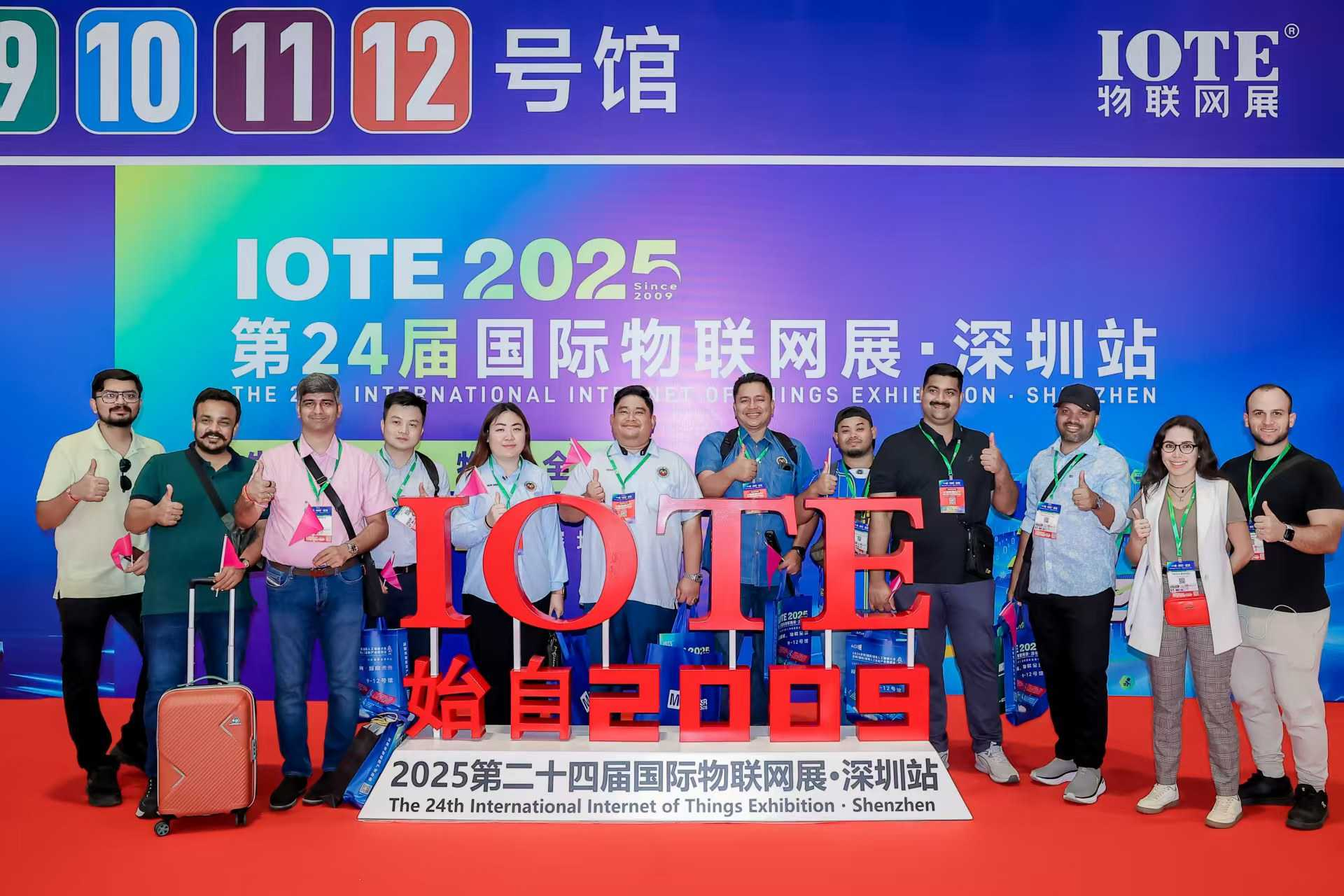
8月27日,IOTE 2025·第24届国际物联网展于深圳国际会展中心(宝安新馆)隆重开幕。本届展会以“生态智能·物联全球”为主题,联合AGIC人工智能展与ISVE智慧商显展,在8万平方米的展区内汇聚超1000家全球展商,涵盖人形机器人、边缘计算、高精度定位、无源物联网、电子纸等前沿领域。开展首日即吸引超5万名专业观众到场,展现出AIoT融合背景下物联网产业的蓬勃活力与无限潜力!
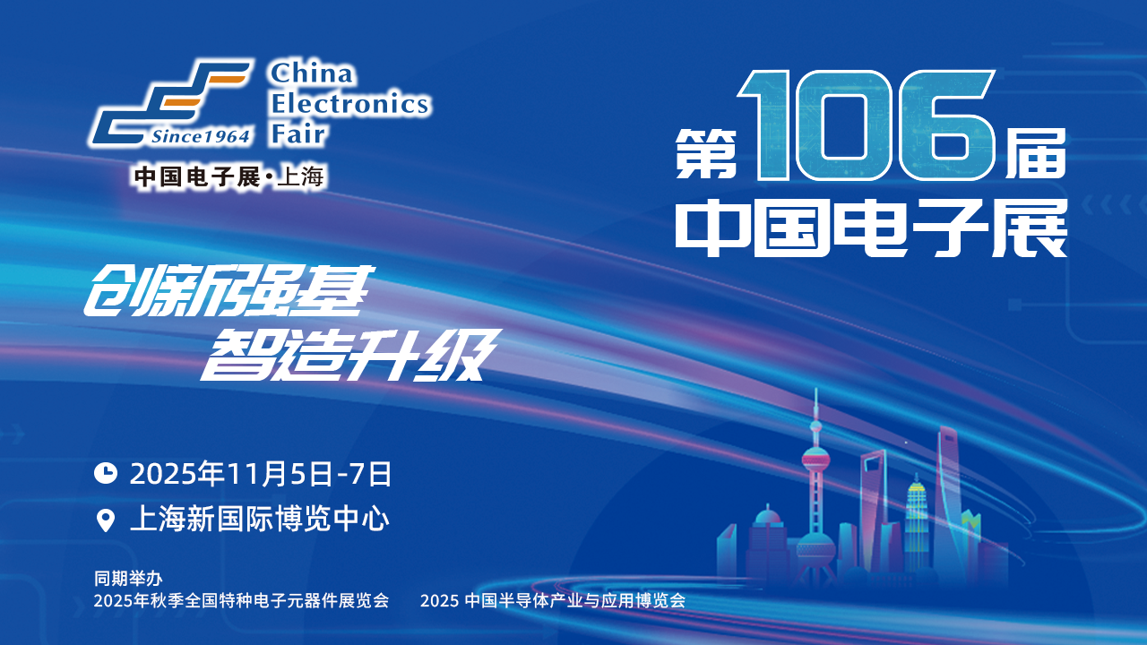
在创新驱动与供给侧改革的持续深化下,2024年中国电子元器件行业迎来强劲复苏与高质量发展,整体销售收入突破2.2万亿元人民币,进出口贸易额稳步增长,展现出显著的发展韧性。行业在移动终端、汽车电子、新能源等关键下游市场的驱动下,不仅产业配套能力实现跃升,一批骨干企业的全球竞争力也持续增强。在此蓬勃发展的产业背景中,第106届中国电子展将于2025年11月5-7日在上海新国际博览中心举行,以“创新强基 智造升级”为主题,搭建全产业链协同创新的重要平台。
寒武纪发布《股票交易风险提示公告》明确指出:当前股价已严重脱离基本面,存在较大投资风险,提醒投资者理性决策,谨慎参与交易。
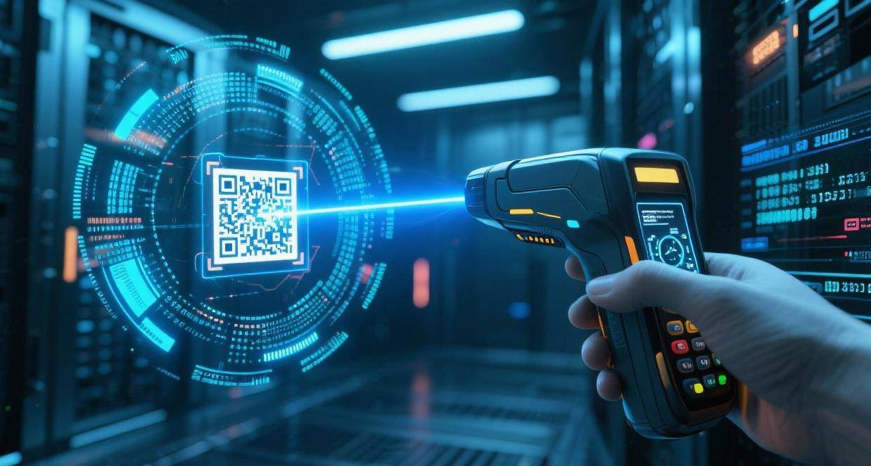
在现代物流体系中,快递驿站作为“最后一公里”的关键节点,其运营效率直接影响用户体验。面对日益增长的包裹处理压力,传统人工登记模式已难以满足高效、精准的操作要求。而搭载智能扫码技术的PDA手持终端,正成为快递驿站实现数字化管理、提升出入库效率的核心工具。


