发布成功

CSW01液位检测芯片
1.1一般特征
1通道电容式触摸传感器,具有灵敏度差校正
低功耗
漏极开路数字输出
上电复位内部电源
嵌入式常见和正常的噪音消除电路
符合RoHS标准SOT-26封装
1.2应用
家电
手机霍尔传感器更换
液位传感
开关更换
薄膜开关更换
人机界面的玩具和游戏互动
密封控制面板,键盘
座椅传感器坐浴盆
1.3原理图
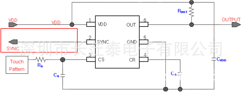
The capacitor and resistor might be connected with CS (pin3) for getting a stable sensitivity.
The capacitor value which is connected to CR pin (CR) should be little bigger than the total CS capacitance (include parasitic capacitance) for touch operation.
CSW01 is reset by internal reset circuit. VDD voltage rising time should be shorter than 100msec for proper operation.
The sensitivity can be adjusted the total CS capacitance and the difference the total CS capacitance and the CR value (Refer to chapter 6.2).
From two CSW01 to ten CSW01 (or other TS series touch sensor) can work on the one application at the same time thanks to SYNC function. (Refer to chapter 6.3)
CSW01 OUT port has an open drain structure. The pull-up resistor should therefore be needed as above figure.
VDD periodic voltage ripples over 50mV or the ripple frequency which is lower than 10 kHz it can cause wrong operation. To prevent above problem, power (VDD, GND) line of touch circuit should be separated from the other circuit. Especially the LED driver power line or digital switching circuit power line should be certainly treated to be separated from touch circuit.
The CS pattern should be routed as short as possible and the width of the line should be around 0.25mm.
The CS pattern routing should be formed by bottom metal (opposite metal of touch PAD).
The capacitor which is between VDD and GND is an obligation. It should be placed as close as possible from CSW01.
The empty space of PCB must be filled with GND pattern to strengthen GND pattern and to prevent external noise that causes interference with the sensing frequency.
行业分类 : 测试设备
开发平台 :
交付形式 :
性能参数 :
应用场景 :